JEDEC Updates HBM2 Memory Standard To 3.2 Gbps; Samsung's Flashbolt Memory Nears Production
by Ryan Smith on February 3, 2020 8:00 PM EST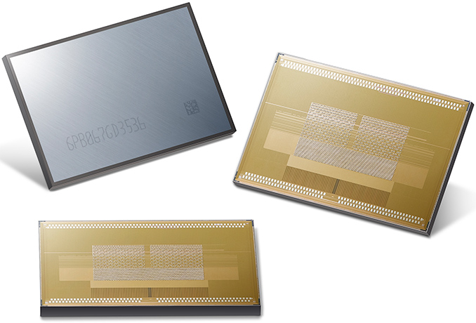
After a series of piecemeal announcements from different hardware vendors over the past year, the future of High Bandwidth Memory 2 (HBM2) is finally coming into focus. Continuing the industry’s ongoing momentum with HBM2 technology, late last month JEDEC published an updated revision of the HBM2 standard. The updated standard added support for even faster memory speeds of up to 3.2Gbps/pin, and in the process pushed the fastest speed for a complete stack of HBM2 memory to 410GB/sec. Meanwhile the memory manufacturers themselves have been preparing for this moment for a while, and Samsung has put out their own matching announcement regarding their Flashbolt HBM2 memory.
First and foremost, let’s dive into the latest version of the HBM2 standard. JESD235C, as it’s officially called, is a relatively small update to the HBM2 standard. After introducing more sizable changes a couple of years back with 12-Hi memory stacks, expanding both the speed and capacity of HBM2 memory, the latest revision is a more measured update focusing on performance.
The biggest change here is that the HBM2 standard has officially added support for two higher data rates, bringing 2.8Gbps/pin and 3.2Gbps/pin into the standard. Coming from the previous standard’s maximum rate of 2.4Gbps/pin, this represents an up-to 33% increase in memory bandwidth in the case of 3.2Gbps HBM2. Or to put this in more practical numbers, a single stack of 3.2Gbps HBM2 will deliver 410GB/sec of bandwidth, up from 307GB/sec in the last standard. Which for a modern, high-end processor supporting 4 stacks (4096-bit) of memory, this brings the aggregate bandwidth available to a whopping 1.64 TB/sec.
| HBM2 Memory Generations | |||||
| JESD235C | JESD235B | JESD235A | |||
| Max Bandwidth Per Pin | 3.2 Gb/s | 2.4 Gb/s | 2 Gb/s | ||
| Max Die Capacity | 2 GB | 2 GB | 1 GB | ||
| Max Dies Per Stack | 12 | 12 | 8 | ||
| Max Capacity Per Stack | 24 GB | 24 GB | 8 GB | ||
| Max Bandwidth Per Stack | 410 GB/s | 307.2 GB/s | 256 GB/s | ||
| Effective Bus Width (1 Stack) | 1024-bit | ||||
| Voltage | 1.2 V | 1.2 V | 1.2 V | ||
All told, this latest update keeps even a single stack of HBM2 quite competitive on the bandwidth front. For comparison’s sake, a 256-bit GDDR6 memory bus with 14Gbps memory can reach 448GB/sec of aggregate bandwidth; so a single stack of HBM2 only slightly trails that. And, of course, HBM2 can scale up to a larger number of stacks more easily than GDDR6 can scale up in bus width, keeping larger HBM2 topologies well ahead of discrete GDDR6 memory chips as far as bandwidth is concerned.
The trade-off, as always, is cost and capacity. HBM2 remains a premium memory technology – due in part to the complexities involved in TSVs and die stacking, and in part to manufacturer product segmentation – and there aren’t currently any signs that this will change. Meanwhile the latest HBM2 standard does not increase memory capacities at all – either through density or larger stacks – so the maximum size of a single stack remains 24GB, allowing a 4 stack configuration to pack up to 96GB of memory.
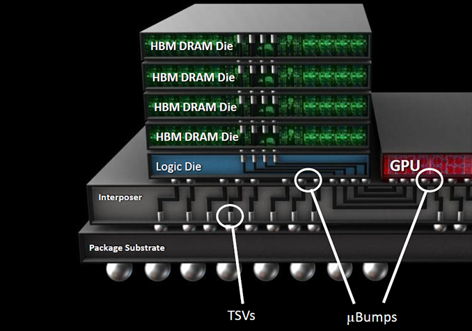
HBM In A Nutshell
Meanwhile, it’s interesting to note that as of JESD235C, JEDEC has backed off just a bit with regards to standardizing HBM2 die stack dimensions. In the previous version of the standard, the dimensions for 12-Hi stacks were listed as “TBD”, but for the new revision the group has seemingly punted on any standardization whatsoever. As a result, there isn’t a single standard height for 12-Hi stacks, leaving it up to memory manufacturers to set their own heights, and for customers to accommodate any differences between the manufacturers.
It is also worth noting that while the HBM2 standard doesn’t directly impose power limits on its own, the standard does specify regular operating voltages. HBM2 since its inception has operated at 1.2V, and the latest standard has not changed this. So the faster memory speeds should come with little (if any) increase in power consumption, as they won’t require higher voltages to drive them.
Finally, it looks like JEDEC has passed on formally adopting the “HBM2E” moniker for the latest memory standard. In pre-standard technology announcements from Samsung, SK Hynix, and others, all of these groups referred to the memory as HBM2E. And indeed, Samsung still is. However this appears to be an entirely informal arrangement, as the official wording on both the JEDEC’s page as well as in the standard itself continue to refer to the memory as HBM2. So it is almost guaranteed that we’re going to see the two terms thrown around interchangeably over the next couple of years.
Samsung Flashbolt Memory Update: Volume Production In H1’2020
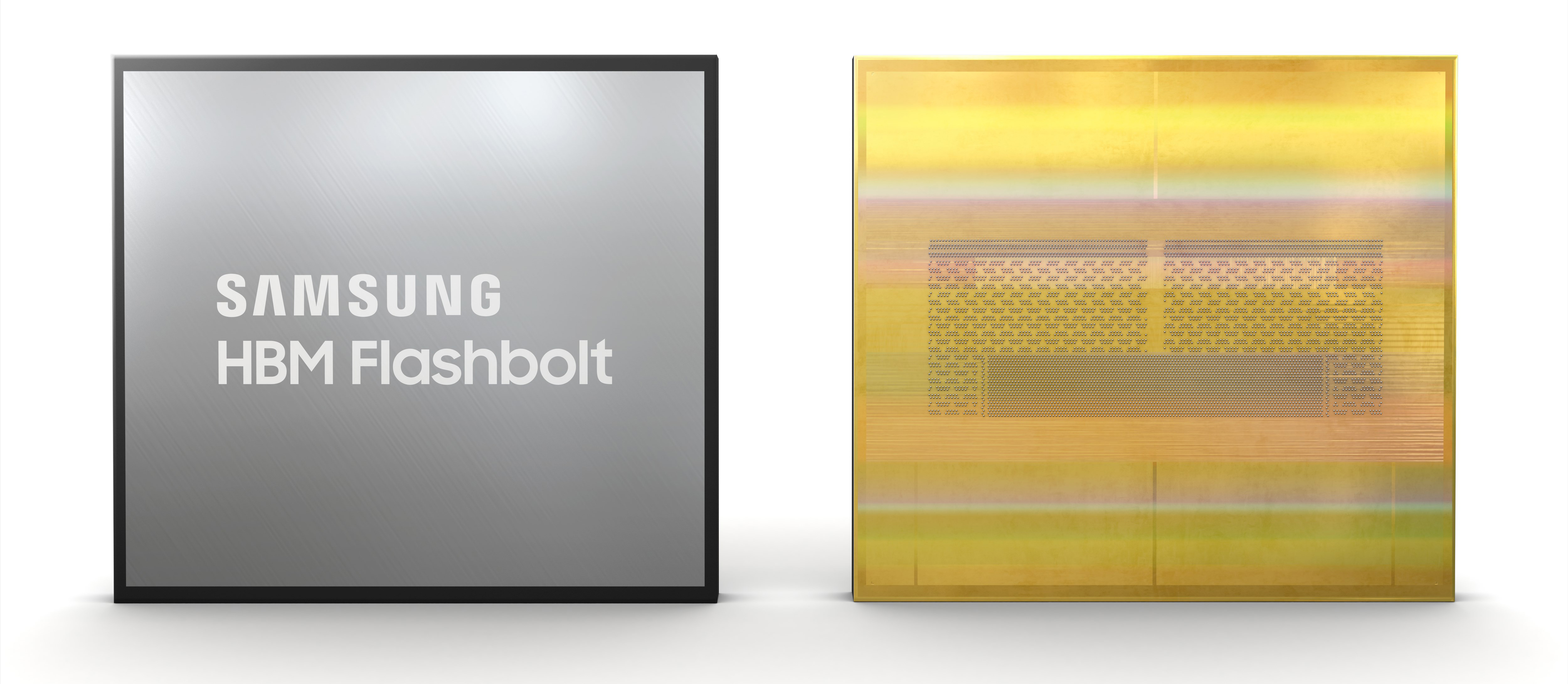
Following the HBM2 standard update, Samsung this afternoon has also issued its own announcement offering an update on the status of their third-generation Flashbolt HBM2E memory. Samsung was the first company to release information on the new speeds, announcing Flashbolt almost a year ago during NVIDIA’s 2019 GPU Technology Conference. At the time Samsung’s announcement was still preliminary, and the company wasn’t saying when they would actually go into mass production. But now we finally have our answer: the first half of this year.
Given that almost a year has passed since the original Flashbolt announcement, Samsung’s announcement is as much a reminder that Flashbolt exists as it is a proper update. Still, today’s announcement offers a bit more detail than Samsung’s relatively high-level reveal last year.
| Samsung HBM2 Memory Comparison | ||||||||
| Flashbolt | Aquabolt | Flarebolt | ||||||
| Total Capacity | 16 GB | 8 GB | 8 GB | 4 GB | 8 GB | 4 GB | ||
| Bandwidth Per Pin | 3.2 Gb/s (4.2 Gb/s OC) |
2.4 Gb/s | 2 Gb/s | 2 Gb/s | 1.6 Gb/s | 1.6 Gb/s | ||
| Number of DRAM ICs per Stack | 8 | 8 | 8 | 4 | 8 | 4 | ||
| DRAM IC Process Technology | 1y | 20 nm | ||||||
| Effective Bus Width | 1024-bit | |||||||
| Voltage | 1.2 V? | 1.2 V | 1.35 V | 1.2 V | ||||
| Bandwidth per Stack | 410 GB/s (538 GB/s OC) |
307.2 GB/s | 256 GB/s | 204.8 GB/s | ||||
Of particular note, Samsung is only announcement 16GB stacks at this time, built using 2GB dies stacked in an 8-Hi configuration. And while this doesn’t preclude Samsung eventually going to 12-Hi, 24GB stacks in the future, it isn’t where the company is going to start at. The memory dies themselves are being manufactured on Samsung’s 1y process technology.
Meanwhile, Samsung appears to be setting some ambitious targets for data rates for Flashbolt. Along with supporting the new 3.2Gbps HBM2 standard, Samsung claims that they are able to go out of spec with Flashbolt, taking the memory to an even speedier 4.2Gbps. This would be a further 31% data rate increase over 3.2Gbps HBM2, and it would push the bandwidth available in a single stack to 538GB/sec, or better than half a terabyte a second. The key word here, of course, is “out of spec”; it’s not clear whether there are any HBM2 memory controllers that will be able to keep up with Samsung’s data rates, and of course there’s the question of power consumption. So while it’s all but guaranteed that Samsung has customers lined up to use Flashbolt at 3.2Gbps, it will be interesting to see whether we see any kind of high-volume products ship at data rates higher than that.
Overall, this makes Samsung the second vendor to announce out of spec HBM2 memory. Last year SK Hynix announced their own HBM2E effort, which is expected to reach 3.6Gbps. So whatever happens, it would seem we’ll now have multiple vendors shipping HBM2E memory rated to go faster than the brand-new 3.2Gbps spec.
Source: Samsung


24 Comments
View All Comments
Dragonstongue - Monday, February 3, 2020 - link
problem is, does anyone or anything use HBM anymore after Radeon and the few Ngreeedia err Nvidia used on GPU stuff?shame as it never quite seemed to live up to the "promises" as there was no denying it had "great potential" somewhere along the line Raja "screwed the pooch" when it came to Radeon overall...great intentions, lead to seemingly poor "in the real world" given results.
That being said, the various Vega, R9 Fury etc once "tuned" supposedly worked outstanding, beyond this, they seemingly chewed up a bunch of power (real or imagined) vs more standard designs...I suppose it was a very good thing they did use HBM memory ^.^
I wonder what AMD is planning in the future to keep power levels to a more "sane" amount and/or to have some sort of properly done "power down when not needed design" seeing as modern GPU are for sure computers in their own right (they have butt load of shaders and such, why can they not help to "on the ms" adjust timings/power use?
finally, all is well and good, but knowing Samsung they are likely to price this very high indeed and maybe maybe not have it running at the best possible speed with lowest possible power therefore heat produced.....still this would lead to some serious serious "firepower" on a fully fledged out product I am sure of it (would hate to see the cost however)
not likely to be in no $200 GPU (not just USD priced) sure would be nice though, if they could have a "lower cost $ and TDP/watt, but stupidly quick gamers card"
Cooe - Monday, February 3, 2020 - link
Yeah. A metric crapton of high end ASIC's & FPGA's. Also, it's still the only game in town for the highest end data center compute GPU's with seriously beefy double precision compute & whatnot (V100, Vega 20). HBM is doing just fine.Kevin G - Tuesday, February 4, 2020 - link
Of those ASICs, there are several highend networking chips that leverage this due to the very nice bandwidth with relatively low latency it provides. The latency side of HBM (vs. GDDR5/6 in particular) is one of its most under values aspects.(Though for lowest latency, large SRAM and TCAM are still necessary for switches but those remain on-die.)
extide - Monday, February 3, 2020 - link
I bet we will continue to see it in the occasional high end gaming GPU -- and this stuff will almost certainly show up in nvidia's next high end tesla product. If they decided to make an 8GB stack, you could make a nice product with only 2 stacks -- especially if you were willing to run it > 3.2Gb/sec mode -- you could get Radeon VIII b/w numbers with half the stacks. That's progress!lilkwarrior - Tuesday, February 4, 2020 - link
You're extremely not accounting for the fact most GPUs of value to the most valuable GPU consumers for GPu companies—pros not gamers looking for $200 cards—want GPUs w/ optimized capabilities for 4K, deep-learning, and of course ray-tracing.Nvidia definitely hasn't been greedy leading to them having 70% of the workstation market & similar share for the gaming market. Ther RTX cards are next-gen cards for gamers while coveted cards for pros—especially for deep-learning, their core competency.
Retycint - Tuesday, February 4, 2020 - link
This whole concept of Nvidia being "greedy" is laughable, considering that both AMD and Nvidia are billion-dollar, profit-maximizing corporations that answer to its shareholders and board of directors. The pricing strategies of both firms represent their best attempt at maximizing profit. Nvidia didn't price their products high because they were "greedy", it's because they had no competition in the high end market. AMD didn't price their products lower because they were benevolent demi-gods who wanted to "save consumers", but because they were competing against the market leader Nvidia and needed to undercut Nvidia's products to persuade consumers to switch.Had the market situation in the past few years been reversed, AMD would have probably price their products similarly, because why would they voluntarily give up profit?
Spunjji - Wednesday, February 5, 2020 - link
But the situation *was* reversed in prior years (Radeon 9800 Pro, HD4870 / 5870 series), and yet AMD never mysteriously added 50%+ to the cost of their high-end products in a single generation.Yes, it's silly to refer to a corporation as "greedy". It's also true, though, that Nvidia's version of fierce competition has involved leveraging their market position to introduce proprietary offerings of dubious value to tie customers to their product stack, then cranking prices up in cycles where competition is lighter.
They're basically the Apple of the GPU market. The iPhone 11 Pro may be an excellent phone and arguably one of the best on the market, but there's no damn way it's worth $1000+ for any reason other than that's what Apple chose to charge for it.
PEJUman - Wednesday, February 5, 2020 - link
I am wondering what is the fraction of ppl buying 11 Pro at full retail asking price. Most US carriers brought back the 2 years contract subsidies during the holiday seasons last year, effectively dropping the 11 Pros by $300-400. And I think there is a healthy amount of '24 months lease' user base with the '0% financing' from carriers and apple themselves.TLDR: I think just like car leasing, the ownership business model for phones might by ending soon. See: "https://www.fool.com/investing/2018/06/08/why-risi...
My speculation is that apple been inflating its phone prices starting in 2017, with the goal to slowly build the residual value of its phones to support 12-24 months lease business model by 2022-23 time-frame. Ultimately transforming itself into a 'hardware&software ecosystem-as-service' behemoth.
Cullinaire - Friday, February 7, 2020 - link
It's worth whatever Apple decided to charge for it, because people chose to BUY IT at that price.Quite simple really.
ksec - Tuesday, February 4, 2020 - link
in the realm of HPC, HBM is cheap. And as we move into more Custom Processor in HPC hopefully HBM will pick up speed with even higher bandwidth.But we dont seems to be severely bandwidth limited in high end Gaming GPU.