Samsung to Produce DDR5 in 2021 (with EUV)
by Anton Shilov on March 25, 2020 7:45 AM EST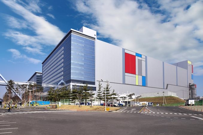
Samsung is on track to start volume production of DDR5 and LPDDR5 memory next year using a manufacturing technology that will take advantage of extreme ultraviolet lithography (EUVL). In fact, Samsung has been playing with EUV-enabled DRAM fabrication process for a while and has already validated DDR4 memory with select partners.
To date, Samsung has produced and shipped a million of DDR4 DRAM modules based on chips made using the company’s D1x process technology that uses EUV lithography. These modules have completed customer evaluations, which proves that Samsung’s 1st Generation EUV DRAM technology enables to build fine circuits. Samsung’s D1x is an experimental EUVL fabrication process that was used to make experimental DDR4 DRAMs, though it will not be used any further, the company said.
Instead, to produce DDR5 and LPDDR5 next year, the company will use its D1a, a highly-advanced 14 nm-class process with EUV layers. This technology is expected to double per-wafer productivity (DRAM bit output) when compared to D1x technology, which indicates that it uses thinner geomtries. Samsung did not reveal whether its D1a also uses other innovations (in addition to EUVL), such as pillar cell capacitors and dual work function layers for buried wordline gates, as anticipated by analysts from TechInsights who believe that scaling DRAM cell transistors and capacitor structures offer limited capability to scale further from current levels.
| Timeline of Samsung DRAM Milestones | ||
| Date | Milestone | |
| 2021 | 4th-gen 10nm-class (1a) EUV-based 16Gb DDR5/LPDDR5 mass production |
|
| March 2020 | 4th-gen 10nm-class (1a) EUV-based DRAM development | |
| September 2019 | 3rd-gen 10nm-class (1z) 8Gb DDR4 mass production | |
| June 2019 | 2nd-gen 10nm-class (1y) 12Gb LPDDR5 mass production | |
| March 2019 | 3rd-gen 10nm-class (1z) 8Gb DDR4 development | |
| November 2017 | 2nd-gen 10nm-class (1y) 8Gb DDR4 mass production | |
| September 2016 | 1st-gen 10nm-class (1x) 16Gb LPDDR4/4X mass production | |
| February 2016 | 1st-gen 10nm-class (1x) 8Gb DDR4 mass production | |
| October 2015 | 20nm (2z) 12Gb LPDDR4 mass production | |
| December 2014 | 20nm (2z) 8Gb GDDR5 mass production | |
| December 2014 | 20nm (2z) 8Gb LPDDR4 mass production | |
| October 2014 | 20nm (2z) 8Gb DDR4 mass production | |
| February 2014 | 20nm (2z) 4Gb DDR3 mass production | |
| February 2014 | 20nm-class (2y) 8Gb LPDDR4 mass production | |
| November 2013 | 20nm-class (2y) 6Gb LPDDR3 mass production | |
| November 2012 | 20nm-class (2y) 4Gb DDR3 mass production | |
| September 2011 | 20nm-class (2x) 2Gb DDR3 mass production | |
| July 2010 | 30nm-class 2Gb DDR3 mass production | |
| February 2010 | 40nm-class 4Gb DDR3 mass production | |
| July 2009 | 40nm-class 2Gb DDR3 mass production | |
Usage of EUVL will enable Samsung (and eventually other memory makers) to reduce (or eliminate) usage of multi patterning, which enhances patterning accuracy and therefore improves performance and yields. The latter will be beneficiary for production of high-performance high-capacity DDR5 chips as they are meant to increase both performance (up to DDR4-6400) and capacity (up to 32 Gbps). Samsung has not officially revealed how many EUV layers do its D1x and D1a process technologies use.
In addition to revealing its EUV-related achievements, Samsung also said that in the second half this year its P2 fab near Pyeongtaek, South Korea, will begin operations later this year. Initially, the facility will ‘make next-generation premium DRAMs’.
Jung-bae Lee, executive vice president of DRAM Product & Technology at Samsung Electronics, said the following:
"With the production of our new EUV-based DRAM, we are demonstrating our full commitment toward providing revolutionary DRAM solutions in support of our global IT customers. This major advancement underscores how we will continue contributing to global IT innovation through timely development of leading-edge process technologies and next-generation memory products for the premium memory market."
Related Reading:
- Samsung Starts Mass Production at V1: A Dedicated EUV Fab for 7nm, 6nm, 5nm, 4nm, 3nm Nodes
- CES 2020: Micron Begins to Sample DDR5 RDIMMs with Server Partners
- Micron’s DRAM Update: More Capacity, Four More 10nm-Class Nodes, EUV, 64 GB DIMMs
- Keysight Reveals DDR5 Testing & Validation System
- SK Hynix Develops First 16 Gb DDR5-5200 Memory Chip, Demos DDR5 RDIMM
- Cadence & Micron DDR5 Update: 16 Gb Chips on Track for 2019
- Cadence and Micron Demo DDR5-4400 IMC and Memory, Due in 2019
Source: Samsung


16 Comments
View All Comments
Anymoore - Wednesday, March 25, 2020 - link
Let's get a few things clear:(1) D1X is three generations behind D1a, like 18 nm vs 14 nm.
(2) The evaluation was done on D1X not D1a, so the D1a process has not been validated yet for production.
(3) The D1X process is almost outdated, as D1Y is mainstream now, and as mentioned, the D1X evaluation will not lead to production.
(4) D1X has no carryover predictability to D1A, the doses and exposure conditions will be significantly different.
Tomatotech - Wednesday, March 25, 2020 - link
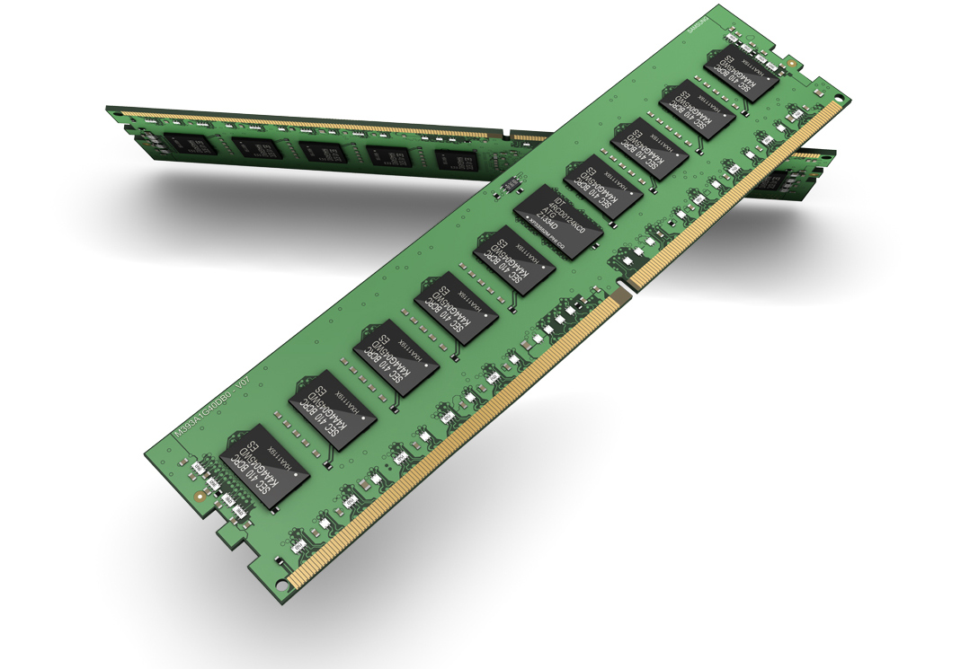
Maybe I'm blind, but that image seems to be of DDR-3 RAM. DDR-4 has a very noticeable curve on the teeth https://www.amazon.co.uk/HP-SDRAM-Memory-Module-Z9...Looking up Google Image search for DDR-4, you can see many images labelled DDR-4 are actually DDR-3, and the differences between the various images.
Ian Cutress - Wednesday, March 25, 2020 - link
It's DDR4. You can tell the connection pins are longer closer to the notch than on the edges.Tomatotech - Wednesday, March 25, 2020 - link
Thanks Ian for clarifying!FreckledTrout - Wednesday, March 25, 2020 - link
You can clearly see there are 280 pins not 240. Im joking, of course I didn't count the pins.InTheMidstOfTheInBeforeCrowd - Wednesday, March 25, 2020 - link
The curved edge connector is not the only telltale sign of a DDR4 DIMM module. Much easier to spot regardless of perspective is the position of the notch, as well as the blank area without contact fingers left of the notch, which clearly spell out its DDR4 (Wikipedia has a handy image which clearly illustrates those distinguishing differences: https://en.wikipedia.org/wiki/DDR4_SDRAM#/media/Fi...azfacea - Wednesday, March 25, 2020 - link
what about GDDR7? do we know anything about that? if GDDR6 was based on DDR4, why do i not hear anything about a DDR5 based graphics solution ? no sign of any R&DEliadbu - Saturday, March 28, 2020 - link
GDDR5 was first used in 2008, so while DDR 4 was came out to the market in 2014 GDDR 6 wasn't used 4 years later in 2018. even if DDR 5 will come out to the market say next year GDDR7 might be out 4-5 years later considering last generation technology advancement.but even if we won't see GDDR7 for few more years GDDR 6 can improve like GDDR 5 improved it speed over the years from initial 3.6 Gbit/s to 9Gbit/s and 12Gbit/s for GDDR5X.
Diogene7 - Wednesday, March 25, 2020 - link
If Samsung is planning to produce 16Gbit (2GB) LPDDR5 chip in 2021 with EUV Lithography, when could we expect 32Gbit (4GB) LPDDR5 chip or even 64Gbit (8GB) LPDDR5 chip (or will it be 64Gbit (8GB) STT-MRAM by then ?)eek2121 - Wednesday, March 25, 2020 - link
This is why I suspect we won’t see full consumer DDR5 platforms prior to 2022. I suspect at least some DDR5 support with Zen 4, but I suspect it will be optional. There are currently no consumer DDR5 parts I am aware of on the market.