Micron Announces 176-layer 3D NAND
by Billy Tallis on November 9, 2020 4:00 PM EST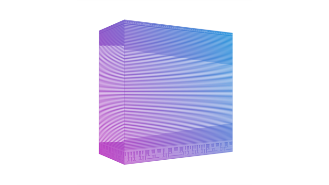
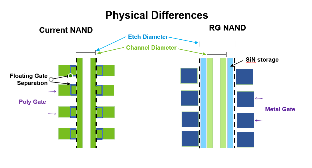
Just in time for Flash Memory Summit, Micron is announcing their fifth generation of 3D NAND flash memory, with a record-breaking 176 layers. The new 176L flash is their second generation developed since the dissolution of Micron's memory collaboration with Intel, after which Micron switched from a floating-gate memory cell design to a charge-trap cell. Micron's previous generation 3D NAND was a 128-layer design that served as a short-lived transitional node for them to work out any issues with the switch to charge trap flash. Micron's 128L flash has had minimal presence on the market, so their new 176L flash will in many cases serve as the successor to their 96L 3D NAND as well.
Micron is still withholding many technical details about their 176L NAND, with more information planned to be shared at the end of the month. But for now, we know their first 176L parts are 512Gbit TLC dies, built using string stacking of two 88-layer decks—Micron would seem to now be in second place behind Samsung for how many layers of NAND flash memory cells they can fabricate at a time, and clearly in first place for the total number of layers on a die.
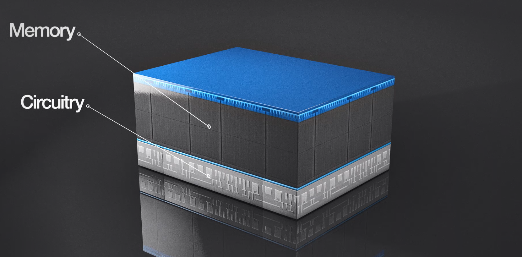
The switch to a replacement gate/charge trap cell design seems to have enabled a significant reduction in layer thickness: the 176L dies are 45µm thick, about the same total thickness as Micron's 64L floating-gate 3D NAND. A 16-die stacked package comes in at less than 1.5mm thick, suitable for most mobile and memory card use cases. As with previous generations of Micron 3D NAND, the chip's peripheral logic is mostly fabricated under the NAND memory cell stacks, a technology Micron calls "CMOS under Array" (CuA). This has repeatedly helped Micron deliver some of the smallest die sizes, and Micron estimates their 176L 512Gbit die is about 30% smaller than the best their competitors currently offer.
The 176L NAND supports an interface speed of 1600MT/s, up from 1200MT/s for their 96L and 128L flash. Read and write (program) latency are both improved by over 35% compared to their 96L NAND, or by over 25% compared to their 128L NAND. Micron cites an overall mixed workload improvement of about 15% for compared to their UFS 3.1 modules using 96L NAND.
Micron's 176L 3D NAND has already started volume production and is shipping in some Crucial-branded consumer SSD products. However, Micron hasn't specified which specific Crucial products are now using 176L NAND (or their 128L NAND, for that matter), so we expect that this is a fairly low-volume release for now. Still, over the next year we should 176L NAND production ramp up to higher volumes than their 128L process ever reached, and we can expect a wide range of products based on this 176L NAND to be released and replace most of what's using their 96L NAND.


29 Comments
View All Comments
Adramtech - Monday, November 9, 2020 - link
30% smaller die? Wow.LiKenun - Monday, November 9, 2020 - link
Maybe we’ll finally get those 2TB SDXC cards or even a 4TB SDUC card. 4TB would mark about ~13 years since the 4GB SDHC card first hit the market.nandnandnand - Monday, November 9, 2020 - link
The 16-die stacked package is 1 TB. So if they can fit two of those in or make larger 1 Tb dies, then a 2 TB microSDXC card is easily possible.I get the impression that the market only cares about microSD. Despite the fact that a full size SD card is several times larger than microSD, the largest capacity available of each type is still 1 TB. Devices that need a full size SD card can use a microSD card inside of an adapter. Still, we are not that far away from having 4 TB microSDUC Express cards, and similar UFS capacities.
martinpw - Monday, November 9, 2020 - link
What are the practical limits on layer count? Curious how much further it is likely to go...Billy Tallis - Monday, November 9, 2020 - link
We're pretty close to the limits of what can be done with a single stack of layers. Almost everyone is now making 3D NAND as two stacks of layers (string stacking), eg. this one is 88+88. That means a lot of manufacturing steps that needed to be done once for early 3D NAND now need to be done twice, plus there's an interface between stacks that needs to be properly aligned and connected. Every roadmap for several hundred layers calls for doing more string stacking of several decks instead of just two. That allows per-die capacity and density to continue increasing, but the manufacturing costs don't scale as dramatically as they did going from eg. 32 through 96 layer nodes.raywin - Monday, November 9, 2020 - link
and this is why i come to this website, thank youstephenbrooks - Monday, November 9, 2020 - link
I was quite curious at what point the whole die height would be filled with solid cells. The statistics on thickness suggest that is quite close. E.g. 176*16 = 2816 layers in a full 16-stack, they're 250nm thick so that's 0.7mm.Adramtech - Monday, November 9, 2020 - link
Micron says it's 1/5 the thickness of a piece of paper. https://www.micron.com/products/nand-flash/176-lay...azfacea - Tuesday, November 10, 2020 - link
yes but they still save steps, they save circuitry, and they will find new ways to save steps. Engineering roadmaps get created as they are used. no body knew about immersion until ppl knew about immersion. whose to say they wont discover new materials new processes along the way that would reduce steps. whose to say they wont exploit multi stacks to get perf the kinds of which has never been seen b4. whose to say they wont revisit the layer limit w. the kind of capital and talent they are going to get with this exponential expansion.the point is the roadmap and pipeline are not dry atm, they are well lubricated, and no other boom has really had or known its roadmap for 10 years later until they many years later. This is not true for HDD whos pipeline has been pretty dry and dead, just compare the HDD growth from 2000s to the one from 2010s, not to mention SSD are shooting at HDD but HDD are not shooting back, they are just trying to hold on to what they can.
rrinker - Tuesday, November 10, 2020 - link
At some point there will be a practical limit as those interface bits start consuming more and more space as the number of layers grows. At some point, the tradeoff of an additional layer won't make up for the loss on each lower layer due to those interconnects, no matter how good the manufacturing process. Question is, is that limit before or after the stack gets too thick to manage for the subsequent stages of the manufacturing process.