3D Packaging
TSMC is no stranger to building big chips. Besides the ~800mm2 reticle limit of their normal logic processes, the company already produces even larger chips by fitting multiple dies on to a single silicon interposer, using their chip-on-wafer-on-substrate (CoWoS) technology. But even with current-gen CoWoS allowing for interposers up to 3.3x TSMC's reticle limit, TSMC plans to build bigger still in response to projected demand from the HPC and AI industries. To that end, as part of the company's North American Technology Symposium last week, TSMC announced that they are developing the means of building super-sized interposers that can reach over 8x the reticle limit. TSMC's current-generation CoWoS technology allows for building interposers up to 2831 mm2 and the company is already seeing customers come...
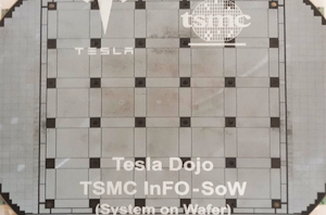
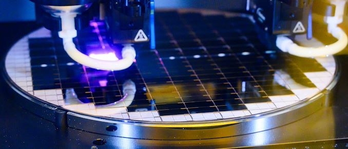
TSMC's System-on-Wafer Platform Goes 3D: CoW-SoW Stacks Up the Chips
TSMC has been offering its System-on-Wafer integration technology, InFO-SoW, since 2020. For now, only Cerebras and Tesla have developed wafer scale processor designs using it, as while they have...
2 by Anton Shilov 6 days ago
Amkor to Build $2 Billion Chip Packaging Fab in Arizona Primarily for Apple
Amkor, the world's second largest independent outsourced semiconductor assembly and test (OSAT) service provider, has announced their intention to build a new advanced chip packaging facility in the U.S...
12 by Anton Shilov on 12/4/2023
TSMC: Short Supply of HPC GPUs to Persist for 1.5 Years
The reports about an insufficient supply of compute GPUs used for artificial intelligence (AI) and high-performance computing (HPC) servers became common in recent months as demand for GPUs to...
6 by Anton Shilov on 9/7/2023
As HPC Chip Sizes Grow, So Does the Need For 1kW+ Chip Cooling
One trend in the high performance computing (HPC) space that is becoming increasingly clear is that power consumption per chip and per rack unit is not going to stop...
40 by Anton Shilov on 6/27/2022_carousel.jpg)
Intel Accelerated Webcast on July 26th: Update on Process Technology and Roadmaps
Earlier this year, new Intel CEO Pat Gelsinger outlined his new ‘IDM 2.0’ vision for Intel. This vision was a three pronged strategy based on improving its own process...
32 by Dr. Ian Cutress on 7/12/2021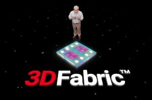
3DFabric: The Home for TSMC’s 2.5D and 3D Stacking Roadmap
Interposers. EMIB. Foveros. Die-to-die stacking. ODI. AIB.TSVs. All these words and acronyms have one overriding feature – they are all involved in how two bits of silicon physically connect...
9 by Dr. Ian Cutress on 9/2/2020_carousel.jpg)
Intel Next-Gen 10-micron Stacking: Going 3D Beyond Foveros
One of the issues facing next-generation 3D stacking of chips is how to increase the density of the die-to-die interface. More connections means better data throughput, reducing latency and...
32 by Dr. Ian Cutress on 8/14/2020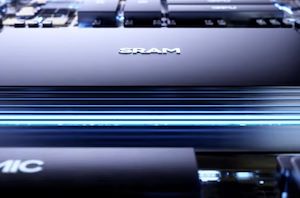
Samsung Announces "X-Cube" 3D TSV SRAM-Logic Die Stacking Technology
Yesterday, Samsung Electronics had announced a new 3D IC packaging technology called eXtended-Cube, or “X-Cube”, allowing chip-stacking of SRAM dies on top of a base logic die through TSVs. Current...
21 by Andrei Frumusanu on 8/14/2020


