Cadence
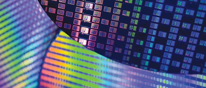
Speaking to partners last week as part of their annual Open Innovation Platform forum in Europe, a big portion of TSMC's roadshow was dedicated to the next generation of the company's foundry technology. TSMC's 2 nm-class N2, N2P, and N2X process technologies are set to introduce multiple innovations, including nanosheet gate-all-around (GAA) transistors, backside power delivery, and super-high-performance metal-insulator-metal (SHPMIM) capacitor over the next few years. But in order to take advantage of these innovations, TSMC warns, chip designers will need to use all-new electronic design automation (EDA), simulation, and verification tools as well as IP. And while making such a big shift is never an easy task, TSMC is bringing some good news to chip designers early-on: even with N2 still a couple...
Cadence Buys Memory and SerDes PHY Assets from Rambus
In a surprising turn of events, Cadence and Rambus entered into a definitive agreement late last week for Cadence to buy memory physical interface IP and SerDes businesses from...
5 by Anton Shilov on 7/24/2023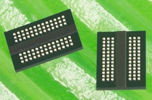
Micron Expects to Debut GDDR7 Memory in 2024
Micron late on Wednesday revealed plans to introduce its first GDDR7 memory devices in the first half of 2024. The memory is expected to be used by next generation...
12 by Anton Shilov on 6/29/2023
Cadence Delivers Technical Details on GDDR7: 36 Gbps with PAM3 Encoding
When Samsung teased the ongoing development of GDDR7 memory last October, the company did not disclose any other technical details of the incoming specification. But Cadence recently introduced the...
29 by Anton Shilov on 3/8/2023
Cadence Cerebrus to Enable Chip Design with ML: PPA Optimization in Hours, not Months
The design of most leading edge processors and ASICs rely on steps of optimization, with the three key optimization points being Performance, Power, and Area (and sometimes Cost). Once...
20 by Dr. Ian Cutress on 7/22/2021New Cadence Transient EM Simulation Tools: 3D Clarity
In the realm of processor and product design, having the right series of tools to actually build and simulate a product has been a key driver in minimizing time...
8 by Dr. Ian Cutress on 10/19/2020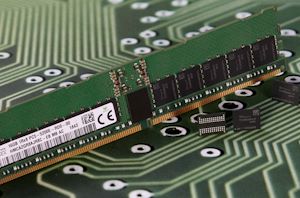
Cadence DDR5 Update: Launching at 4800 MT/s, Over 12 DDR5 SoCs in Development
JEDEC still has not published the DDR5 specification officially, yet it looks like DRAM makers and SoC designers are preparing for the DDR5 launch at full steam. Cadence, which...
20 by Anton Shilov on 3/27/2020
Samsung’s 5nm EUV Technology Gets Closer: Tools by Cadence & Synopsys Certified
Samsung Foundry has certified full flow tools from Cadence and Synopsys for its 5LPE (5 nm low-power early) process technology that uses extreme ultraviolet lithography (EUV). Full flow design...
13 by Anton Shilov on 7/8/2019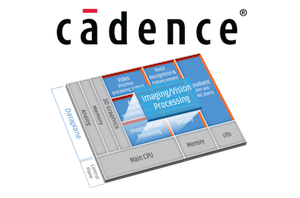
Cadence Announces Tensilica Vision Q7 DSP
Last year we saw the announcement of Cadence’s Tensilica Q6 DSP IP which promised a new architecture that brings integration between vision DSP workloads and new optimised machine learning...
0 by Andrei Frumusanu on 5/15/2019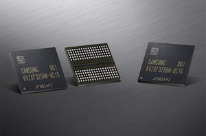
Cadence Tapes Out GDDR6 IP on Samsung 7LPP Using EUV
Cadence has announced that it has successfully taped out its GDDR6 IP on Samsung’s 7LPP fabrication process. The new building blocks should enable developers of various chips to be...
11 by Anton Shilov on 11/26/2018
Cadence & Micron DDR5 Update: 16 Gb Chips on Track for 2019
Earlier this year Cadence and Micron performed the industry’s first public demonstration of next-generation DDR5 memory. At a TSMC event earlier this month the two companies provided some updates...
18 by Anton Shilov on 10/17/2018
Cadence Announces The Tensilica DNA 100 IP: Bigger Artificial Intelligence
Cadence is an industry player we don’t mention nearly enough as much as we should - they make a lot of IP and specialises in accelerator blocks which augment...
9 by Andrei Frumusanu on 9/19/2018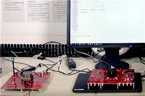
Cadence and Micron Demo DDR5-4400 IMC and Memory, Due in 2019
Cadence this week introduced the industry’s first IP interface in silicon for the current provisional DDR5 specification developed by JEDEC. Cadence’s IP and test chip us fabricated using TSMC’s...
31 by Anton Shilov on 5/3/2018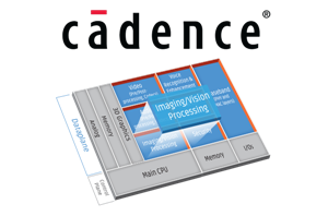
Cadence Announces Tensilica Vision Q6 DSP
Today’s announcement comes from Cadence, and we see the unveiling of a new DSP IP called the new Tensilica Vision Q6. The Q6 succeeds the Vision P6 which as...
20 by Andrei Frumusanu on 4/11/2018
TSMC Teams Up with ARM and Cadence to Build 7nm Data Center Test Chips in Q1 2018
TSMC has announced plans to build its first test chips for data center applications using its 7 nm fabrication technology. The chip will use compute cores from ARM, a...
12 by Anton Shilov on 9/14/2017


